| bobeager.uk | Projects |
|
|
This page is intended to show projects that I have played with (and possibly completed). Currently, these are:
(Raspberry Pi based computer with SSD)The Pironman 5 is nominally just a case for the Raspberry Pi 5. However, it's much more than that. It incorporates I/O expansion, extensive cooling, lighting, and provision for an M.2 SSD. There is also another version, the Pironman 5 Max (not shown here) which is very similar, but provides for two M.2 SSDs; it is also black, with dark acrylic sides! I have put together Two Pironman 5 systems, and one Pironman 5 Max. The Max is not shown here because I didn't take separate pictures. 
The obvious items needed were a Raspberry Pi 5 (I got an 8GB one, but regretted not going for a 16GB one (I did put one of those in the Max), a 1TB SSD, the actual Pironman 5 kit, a power supply (27W for safety) and some cables.The item in the centre is an official backup battery, but it turns out that the Pironman 5 includes all you need for that. I also included a USB SSD reader/writer, and I didn't need that either. 
This is what you get in the kit (plus, the Raspberry Pi, which is not included). Note the screwdriver (I used my own) and the useful spanner (which is definitely needed, at least for the large end, which does the power button). The case (top right) is disassembled into two parts for the build. 
Here, the Raspberry Pi has been mounted in the main part of the case. The half height panel at the back is fitted with the power button, and the extender for the normal micro SD card. At the front, the network and USB ports are presented normally, and the board to the left presents the USB-C power input and two HDMI ports (these are converted to standard size ones). The battery can be seen at top left. The ribbon cable will be connected to the SSD adaptor. 
The SSD adaptor has been fitted on the left, together with the SSD itself. The fairly massive tower cooler has been clamped down on the main chips, interposed with the thermal pads supplied. 
This gives a clear view of the SSD adaptor. The micro SD card slot, and the power button, are also visible here. The micro SD extender can also be seen at bottom left. 
The other part of the case (now fitted with the rear panel fans) has been offered up and screwed together. Note particularly that a vertical extender has been added to the Raspberry Pi GPIB connector, bringing it out to an accessible position. This will be clearer later. 
The GPIB extender can be seen to the left. ")
The transparent acrylic panels have now been fitted, and the adhesive pads (which act as 'feet'). Note the GPIB connector, accessible through the slot in the side panel. A small graphical display can be added to this, and hangs on the side of the case. ")
This view shows the acrylic front panel. Note also the black rectangle at bottom right; this is the programmable matrix display. Not visible are the coloured LEDs inside the top of the case, which help to illuminate the inside. Their effect can, however, be seen in later images. 


These images show the unit powered up and running. The lighting and fans are programmable. The matrix display is visible in some images; by default it shows disk and CPU usage, as well as some other information. One image includes a banana, for scale. PiDP-10 (PDP-10 replica with KA-10 console)The Digital Equipment Corporation (DEC) produced a series of computers (originally called Programmed Data Processors). The early ones were named as PDP- followed by various numbers. Most people think of the PDP machines as being exclusively minicomputers; however, the PDP-10 was arguably a mainframe. Later on, it was renamed the DECsystem-10 (to be succeeded by the DECsystem-20). This was a 36 bit machine, and was a monster compared to the other PDP systems. However, the PDP-10 did show its minicomputer roots, at least in the earliest model, the KA-10. It still had the array of indicator lights on the control panel (over 100 of them), and a large number of switches for data entry, address entry, and various control functions. I used a KA-10 for a year back in the 1970s, and did some assembler programming on it. A kit (PCB, case, LEDs and other parts) is now available to build a replica PDP-10. This was realised by using a Raspberry Pi running emulator software, with the GPIO interface being used to drive the lights, read keyswitches and so on. I am in the process of building one of these. I will document progress here. The kitThe kit arrived! The following is quite detailed, as I was one of the early constructors (serial number 19); I wanted to give an account of what I did to help others. The following picture shows the component parts laid out on my workbench. It can be seen that the PCBs are quite large, so I made sure that there was plenty of room on the bench before I started. I tried to keep as little on the bench as possible, throughout. The decision was made to include all additional connectors and options from the start, to reduce the number of times that things had to be taken apart to solder something new. Thus, there were a number of additional components which are not shown here:

Before construction started, the Raspberry Pi was prepared. I used a Raspberry Pi 5, with 8GB of memory. This is probably overkill, but means that the Pi can be used for other things at the same time as running the PiDP-10. To avoid overheating and possible throttling, the official active cooler was attached. Kapton tape was used to insulate the metal housings on the Ethernet and USB connectors, in case they contacted the LED board. The heat sink on the active cooler was in no danger of making the same kind of contact. The software was installed and tested. 
For construction, I used 63/37 Sn/Pb solder throughout, as it has a slightly lower melting point, which is actually a point and not a range. Given that there were over 1000 joints to make, I set up my extraction/filter fan! Work started with soldering 74 diodes to the smaller board (the one that would later receive the switches). This was straightforward and uneventful. This was followed by the addition of one diode to the larger board (the one for the LEDs), as well as 26 resistors. Then came the connector for the Raspberry Pi GPIO interface, being careful to place this on the rear of the board. The three IC sockets supplied with the kit were then added, and also a fourth one for the optional RS-232 level converter circuit. In the photograph, resistors (bottom, and top right) and IC sockets (top right) have been added. The left hand socket (and the adjacent capacitors) are for the RS-232 level shifting circuit, which is a standalone circuit. I chose to use a MAX202 rather than a MAX232, which meant I could use 0.1µF ceramic capacitors rather then larger polarised parts. This turned out to be important for clearance later on. The additional IC socket was what I usually use; a machined/turned pin part. I was later to wish that I'd fitted such sockets for all of the ICs (see later). The LEDs were initially fitted by dropping them all into place, adding a retainer shield, taping that temporarily, then turning the board over and soldering (all one leg, then a double check and any adjustment, then the other LED). I fitted temporary standoffs in all eight mounting holes to make it easier to keep the LEDs in place without the leads being pushed back through; I used 20mm nylon parts. The retainer shield is a permanent feature, to reduce light bleed-through between LEDs, and is meant to be an interference fit on the LEDs. Due to manufacturing tolerances, it was initially quite loose. However, once the LEDs were soldered in place and did not 'give', it tightened up. A pair of angled pin headers were fitted, one to each board, for connecting the boards together. The cable for this was wider than the connectors, by one pair of holes; the correct blanking plugs were fitted to the cable ends to eliminate any errors in the future due to misalignment of the two ends. A third angled header was also fitted on the reverse side, for connection to the optional maintenance panel. A number of connectors (some optional) were also added to the rear of the board. These were:
Two 5x2 double row angled connectors were also added to the switch board, for optional Spacewar controllers. This is the bench during installation of the LEDs. Note the temporary standoffs so that the LEDs can be dropped into place.

This is the (nearly) completed LED board. The LED shield is omitted for clarity. Other items of note:

Finally, the two DE-9 connectors (for serial ports) were bolted in place. 5mm spacers were used under the mounting lugs, as they do not sit flush with the LED board. Connections were made from these, to the RS-232 pins on the level shifter circuit, unfortunately on the other side of the board. The Raspberry Pi was also installed, using nylon standoffs attached to the LED board with metal screws. Nothing was attached to the free ends of the standoffs at this stage. 

Attention was then turned to the switch board; here it is, before adding the 74 switches. There are 74 diodes, one for each switch; also the right angled header for connection to the display board, via a cable. Still to be added are the two right angled connectors (bottom left) for the optional Spacewar controllers. The plastic boxes contain the switches, 74 of them! The third and fifth boxes contain momentary switches (more correctly known as keys on a PDP-10), and the others contain normal switches (known as switches on a PDP-10). 
The switches were first tacked in place by soldering one mounting pin. Care was taken to distinguish momentary switches, or keys, from the rest. Positions were then checked and adjusted before soldering the other pins, doing one pin on all switches before returning for the next one (to avoid overheating any of them). It was found that a lot of the pins (particularly the mounting ones) did not want to 'take' solder, so extra flux was applied via a flux pen. The board was then cleaned of excess flux. 
The fully loaded switch board was surprisingly heavy. Care had to be taken to support it when handling, to avoid undue flexing. The LED board and the switch board were connected up and a final run of the LED/switch test program was carried out. All was well. The switch board was installed into the black baseplate, which provides protection. 
The protective film was removed from the front of the acrylic printed front panel, and it was pushed into place in the main case. This was followed by the LED board, secured with eight self tapping screws (first ensuring that the LED shield/retainer was in position). The ribbon cable was attached to the LED board. The baseplate (containing the switch board was offered up, and the ribbon cable was attached to that too. The baseplate was attached to the main case with four self tapping screws. 
The back panel was then prepared. It is made of multiple parts; see below. Parts C and D are used to join parts A and B; it was important to use nylon nuts and bolts due to the small clearance to the LED board, which causes a risk of short circuits if metal components are used. Part B has two fan mounting positions, but only the left hand one was used (the other area being left free for the maintenance panel). Three breakout parts were removed:
Issues have been reported with insufficient space between the LED board and the back panel, one in particular being the lack of depth for the heads of bolts holding the fans in place. I chose to mount the fans with rubber fan mounts; not only are they quite flat, but they are made of rubber, so there is no risk of a short circuit. An enlarged image of one of these mounts is shown below, and four of them can be seen attached to part B. Before assembling the components of the rear panel, part B was first fitted in place to check clearances. There were no issues. However, part A, while fitting everywhere else, did not 'sit' correctly at the bottom left corner, due to the presence of the two whit JST XH connectors (these were chosen because the fans are fitted with the corresponding connector). 

(to be continued)PiDP-8 (PDP-8/I replica)The Digital Equipment Corporation (DEC) produced a series of computers (originally called Programmed Data Processors). The early ones were named as PDP- followed by various numbers. To me, one of the most interesting was the PDP-8, a machine using a 12-bit word (no bytes). It had a mere 3 bits to specify an instruction, and a maximum of 32k words of memory. It was originally produced using discrete logic; this was superseded by an integrated circuit version using logic circuits with just a few gates per chip. The first IC model was the PDP-8/I. A distinguishing feature of the PDP-8/I was the large number of indicator lights, that showed a great deal of what was going on - at quite a low level. The machine had only eight basic opcodes, and eight indicators were dedicated to showing the opcode of the current instruction! Others showed instruction phases, and of course some showed the contents of the accumulator, memory address register and so on (other models used fewer lights, and used a rotary switch to select what was displayed). A kit (PCB, case, LEDs and other parts) was available to build a replica PDP-8/I. This was realised by using a Raspberry Pi running emulator software, with the GPIO interface being used to drive the lights, read keyswitches and so on. I built one of these; pictures below. The worst part was soldering 89 LEDs, and 26 switches! It includes a number of different boot options; console access can be via the Raspberry Pi's serial port, but I decided that it would be neater to access the PiDP-8 console using ssh over wi-fi. The Raspberry Pi in the PiDP-8 runs a version of Linux, but I am looking into replacing that with FreeBSD, as that would be easier for me to maintain. To do this, some of the emulator code will need to be rewritten so that it uses the FreeBSD model for access to the GPIO bus. There is some clever multiplexing which is used to drive all of the LEDs from a limited number of GPIO pins (as well as sampling the switches), so I will need to replicate that. 
Front of the circuit board, with switches, LEDs, etc. 
Rear of the circuit board, including the Raspberry Pi. The wood is used to mount the board into the case! 
The completed PiDP-8 on the bench. SBC6120 (PDP-8 replica)As noted above (but repeated here) the Digital Equipment Corporation (DEC) produced a series of computers (originally called Programmed Data Processors). The early ones were named as PDP- followed by various numbers. As stated above, one of the most interesting was the PDP-8, a machine using a 12-bit word (no bytes). It had a mere 3 bits to specify an instruction, and a maximum of 32k words of memory. It was originally produced using discrete logic; this was superseded by an integrated circuit version using logic circuits with just a few gates per chip. Eventually, an entire PDP-8 CPU appeared in a single chip, the Intersil/Harris 6100, with a later version being the 6120. A kit (PCB and difficult-to-obtain chips) was available to build a single board PDP-8 using the Harris 6120; this was called the SBC6120. I built one of these; pictures below. It includes a ROM monitor for booting, testing, etc. I later burned custom ROMs that worked better for me. 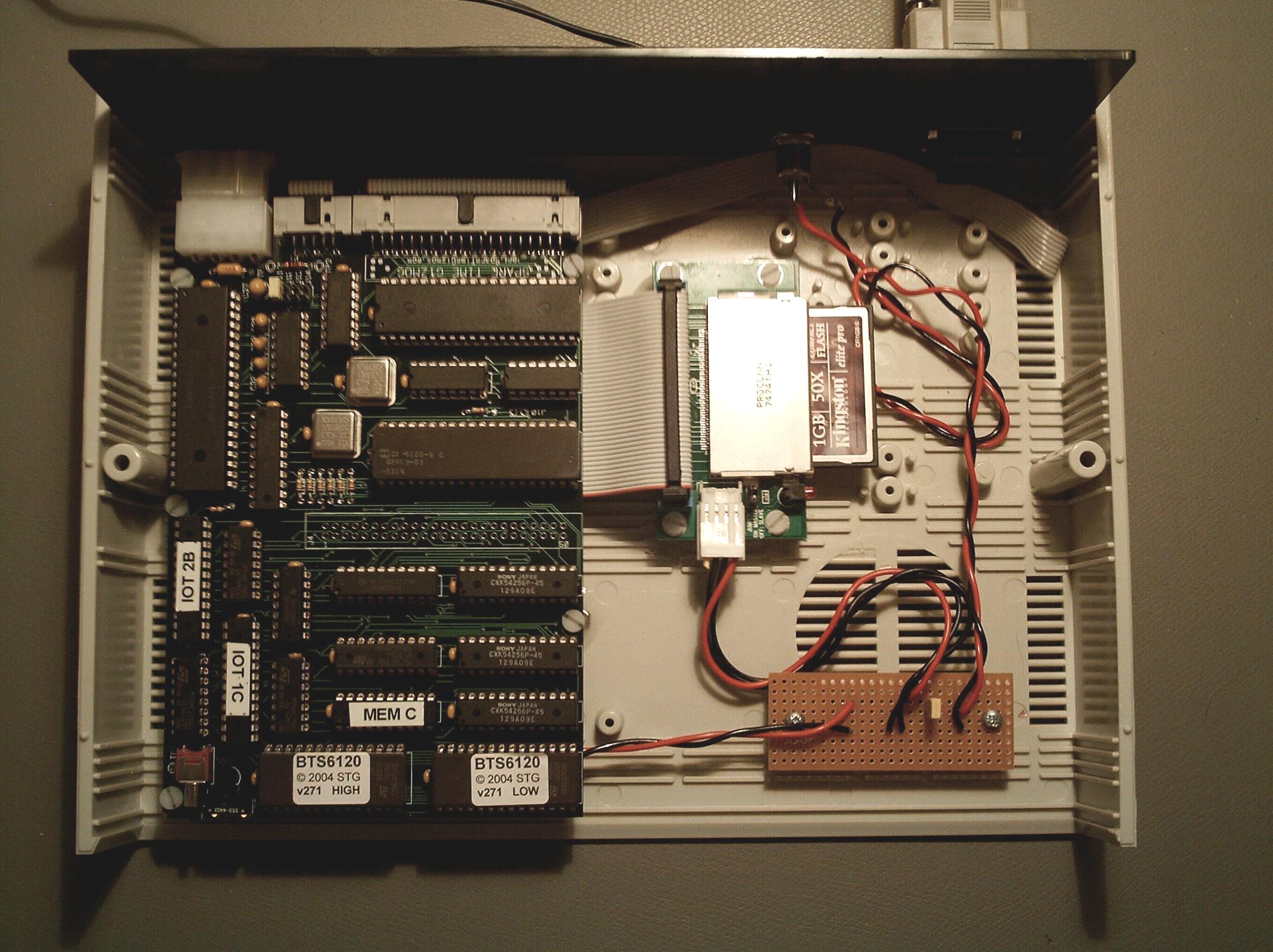
Interior of the basic SBC6120. The small board is for power isolation and testing. 
Another view of the basic SBC6120. This shows the power connector on the rear panel, and the DE9 connector for the serial (console) port. I later built a second one, this time with a silk screened front panel, LEDs and switches. I put it in a basic wooden case. The DE9 console connector, and the power sockets, are mounted in a plate on the side. The rear panel is attached with magnets, to make it easy for enthusiasts to look inside! A picture follows. 
A view of the enhanced SBC6120, including front panel, LEDs and switches. Both of these machines use a Compact Flash card as multiple 2MB hard disks, and will run the disk operating system known as OS/8. They can compile and run programs in various languages, including BASIC, FOCAL and FORTRAN. Voice over IP PBXOne of the most useful projects was the Voice over IP PBX (Private Branch Exchange). This is a mini telephone exchange, within the house. The house is large and slightly rambling, so an internal phone system is very useful. Of course, all phones also work externally as well, so phone calls can be made from almost any room. The PBX is based on an HP microserver, an inexpensive, small, low power PC. The underlying software is the open source Asterisk system, running on the FreeBSD operating system (not Linux). 
An HP microserver The system is connected to the normal POTS telephone system via a LinkSys/Cisco SPA3102 ATA, which provides the necessary FXO port, as well as an FXS port that is used for an external bell. 

An SPA3102 All of the actual phones are of course IP phones. Most are LinkSys/Cisco SPA303 models, with two being the smaller SPA301. These all plug directly into the house gigabit network. 

An SPA301 phone (left) and an SPA303 (right) For the history of telephone systems in the house, see my presentation on the subject. DoorbellThe house is big, and it has a strange layout. This means that it isn't possible reliably to hear a knock at the door everywhere in the house. It certainly can't be heard in the garden. One option that was considered was a pair of cord-operated butlers' bells, with the cords tied together - but that would only have been a partial solution. It was decided to harness the house PBX. The solution adopted was as follows:
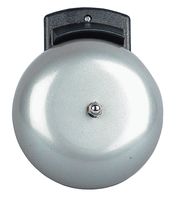
The bell used in the garden |
|
![]()

This site is copyright
© 2025
Bob Eager
Last updated:
03 Dec 2025